| CPC H01L 27/1225 (2013.01) [G02F 1/1368 (2013.01); G02F 1/13306 (2013.01); G02F 1/136209 (2013.01); H01L 27/1251 (2013.01); H01L 27/1259 (2013.01); H01L 29/24 (2013.01); H01L 29/41733 (2013.01); H01L 29/42384 (2013.01); H01L 29/4908 (2013.01); H01L 29/517 (2013.01); H01L 29/7869 (2013.01); H01L 29/78633 (2013.01); H01L 29/78675 (2013.01); G02F 1/13685 (2021.01); G02F 2202/10 (2013.01); G02F 2202/104 (2013.01); H10K 59/1213 (2023.02)] | 9 Claims |

|
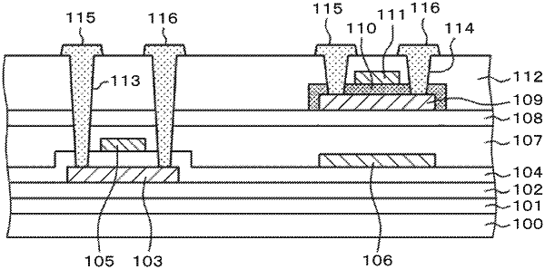
1. A display device comprising;
a substrate having a display region in which pixels are formed and peripheral region in which a drive circuit is formed,
an oxide semiconductor layer, and
a silicon semiconductor layer,
wherein
the pixels include a first TFT having the oxide semiconductor layer,
a first gate electrode of the first TFT is arranged above the oxide semiconductor layer,
a first insulating film is arranged between the oxide semiconductor layer and the first gate electrode, and covers a side surface of the oxide semiconductor layer,
a passivation film is formed on the first gate electrode and the first insulating film,
a first electrode is connected to a drain of the first TFT via a first through hole formed in the first insulating film and the passivation film,
a second electrode is connected to a source of the first TFT via a second through hole formed in the first insulating film and the passivation film,
the drive circuit includes a second TFT having the silicon semiconductor layer,
the second TFT has a second gate electrode and a second insulating film,
an interlayer insulation film is formed between the oxide semiconductor layer and the silicon semiconductor layer, and
a metal film under the first TFT is formed on a same layer where the second gate electrode of the second TFT is formed.
|