| CPC H01L 27/0805 (2013.01) [H01L 23/5222 (2013.01); H01L 23/5386 (2013.01); H01L 24/14 (2013.01); H01L 28/60 (2013.01)] | 20 Claims |
|
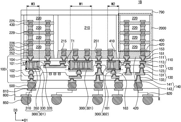
1. A semiconductor package comprising:
a redistribution substrate;
a package substrate, below the redistribution substrate, comprising a first metal line;
a first solder pattern between the redistribution substrate and the package substrate;
a first passive device in the redistribution substrate, the first passive device comprising a first terminal and a second terminal; and
a first semiconductor chip on a top surface of the redistribution substrate, the first semiconductor chip vertically overlapping at least a portion of the first passive device,
wherein the redistribution substrate comprises:
a dielectric layer in contact with a first lateral surface, a second lateral surface opposite to the first lateral surface, and a bottom surface of the first passive device;
a lower conductive pattern on the first terminal;
a lower seed pattern provided between the first terminal and the lower conductive pattern, and directly connected to the first terminal;
a first upper conductive pattern on the second terminal;
a first upper seed pattern provided between the second terminal and the first upper conductive pattern, and directly connected to the second terminal; and
a first redistribution pattern laterally spaced apart from the first passive device without being connected to the first passive device, and
wherein the first metal line in the package substrate is connected to the first redistribution pattern in the redistribution substrate through the first solder pattern.
|