| CPC H01L 27/0664 (2013.01) [H01L 27/0727 (2013.01); H01L 29/36 (2013.01); H01L 29/4236 (2013.01); H01L 29/7395 (2013.01); H01L 29/7397 (2013.01)] | 12 Claims |
|
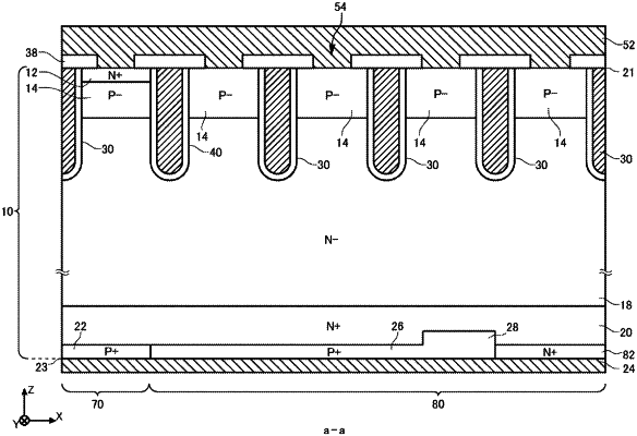
1. A semiconductor device, comprising:
a semiconductor substrate that includes a first conductivity type drift region;
a transistor portion that includes a first conductivity type emitter region having a doping concentration higher than the drift region in a region which is in contact with an upper surface of the semiconductor substrate; and
a diode portion that includes a first conductivity type cathode region having a doping concentration higher than the drift region in a region which is in contact with a lower surface of the semiconductor substrate, and is arranged side by side with the transistor portion in a preset arrangement direction in an upper surface of the semiconductor substrate; and
a second conductivity type lower surface region that is provided in a region other than the cathode region in a region which is in contact with the lower surface of the semiconductor substrate,
wherein the lower surface region includes a thick portion in which an end portion in a top view has a larger thickness in a depth direction of the semiconductor substrate than other portions.
|