| CPC H01L 27/0629 (2013.01) [H01L 21/0254 (2013.01); H01L 21/8252 (2013.01); H01L 27/0605 (2013.01); H01L 29/2003 (2013.01); H01L 29/40 (2013.01); H01L 29/66212 (2013.01); H01L 29/66462 (2013.01); H01L 29/7786 (2013.01); H01L 29/872 (2013.01)] | 5 Claims |

|
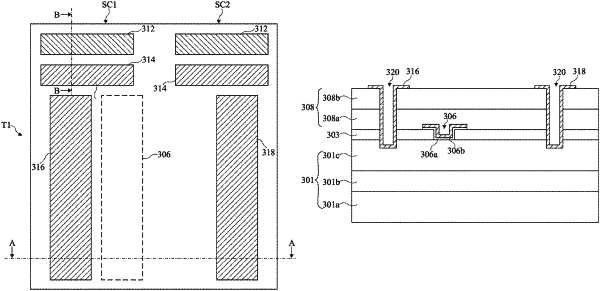
1. An electronic component comprising:
gallium nitride substrate;
an aluminum-gallium nitride layer;
first and second connection terminals on the gallium nitride substrate;
a field-effect power transistor on the gallium nitride substrate and including a gate structure, source, and drain, the gate structure being directly on the gallium nitride substrate and includes a gate dielectric layer and a gate electrode;
a passivation layer on the gate structure of the field-effect power transistor;
a first Schottky diode on the gallium nitride substrate and coupled between and to both the first connection terminal and the gate electrode of the field-effect power transistor; and
a second Schottky diode on the gallium nitride substrate and coupled between and to both the second connection terminal and the gate electrode of the field-effect power transistor, the source and drain of the field-effect power transistor and cathode terminals of each of the first Schottky diode and the second Schottky diode are in respective trenches extending in the passivation layer to the gallium nitride substrate, anode terminals of each of the first Schottky diode and the second Schottky diode are in respective trenches extending in the passivation layer to the aluminum-gallium nitride layer.
|