| CPC H01L 27/0605 (2013.01) [H01L 21/8252 (2013.01); H01L 29/2003 (2013.01); H01L 29/66212 (2013.01); H01L 29/66219 (2013.01); H01L 29/66462 (2013.01); H01L 29/7786 (2013.01); H01L 29/7787 (2013.01); H01L 29/872 (2013.01)] | 17 Claims |
|
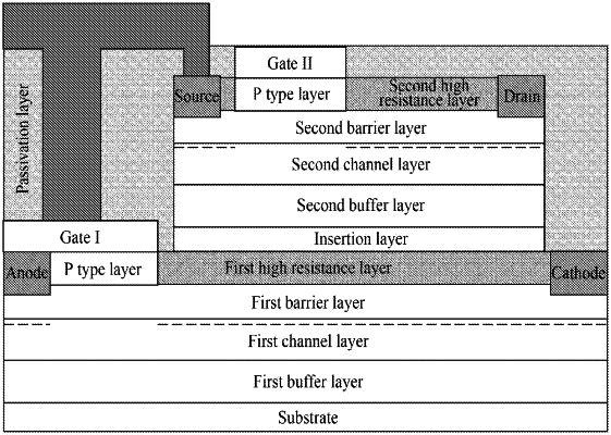
1. A group III nitride transistor structure capable of reducing a leakage current, comprising:
a first heterojunction and a second heterojunction which are laminated, wherein the first heterojunction is electrically isolated from the second heterojunction via a high resistance material or insertion layer;
a first electrode, a second electrode and a first gate which are matched with the first heterojunction, wherein the first electrode is electrically connected with the second electrode via a first two-dimensional electron gas in the first heterojunction, and a third semiconductor is arranged between the first gate and the first heterojunction, wherein the third semiconductor can exhaust a part of the first two-dimensional electron gas located below the third semiconductor, and the first gate is also electrically connected with the first electrode;
a source, a drain and a second gate which are matched with the second heterojunction, wherein the source is electrically connected with the drain via a second two-dimensional electron gas in the second heterojunction, and the source and the drain are also electrically connected with the first gate and the second electrode respectively, a sixth semiconductor is arranged between the second gate and the second heterojunction, wherein the sixth semiconductor can exhaust a part of the second two-dimensional electron gas located below the sixth semiconductor.
|