| CPC H01L 25/0753 (2013.01) [H01L 27/1214 (2013.01); H01L 33/0093 (2020.05); H01L 33/22 (2013.01); H01L 33/62 (2013.01); H01L 2933/0066 (2013.01)] | 15 Claims |
|
1. A manufacturing method of a light emitting element, the method comprising:
preparing a lower substrate comprising a substrate and a buffer semiconductor layer formed on the substrate;
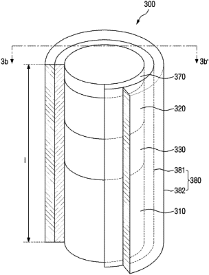
forming an element rod by forming a separating layer on the lower substrate; forming a first conductivity type semiconductor layer, an active material layer, and a second conductivity type semiconductor layer on the separating layer; and etching the first conductivity type semiconductor layer, the active material layer, the second conductivity type semiconductor layer, and the separating layer in a direction perpendicular to an extension direction of the lower substrate;
forming a first insulating layer surrounding an outer peripheral surface of the element rod;
forming a second insulating layer surrounding an outer peripheral surface of the first insulating layer; and
separating the element rod from the lower substrate to form a light emitting element by etching and removing the separating layer by an etchant for separation comprising fluorine (F),
wherein the first insulating layer comprises at least one of silicon oxide (SiOx), aluminum oxide (Al2O3), or silicon oxynitride (SiOxNy), and the second insulating layer comprises at least one of silicon nitride (SiNx), aluminum nitride (AlN), or silicon oxynitride (SiOxNy),
wherein the forming of the first insulating layer comprises:
forming a first insulating layer disposed to cover an outer surface of the element rod; and
a first etching step of exposing a top surface of the element rod by etching the first insulating layer, and
wherein the forming of the second insulating layer comprises:
forming a second insulating layer disposed to cover the outer surface of the element rod; and
a second etching step of exposing the top surface of the element rod by etching the second insulating layer; and
wherein the second insulating layer has an etch selectivity with respect to the etchant, which is greater than an etch selectivity of the first insulating layer with respect to the etchant.
|