| CPC H01L 25/074 (2013.01) [H01L 25/0657 (2013.01); H01L 25/18 (2013.01); H01L 25/50 (2013.01); H01L 24/29 (2013.01); H01L 24/32 (2013.01); H01L 29/66742 (2013.01); H01L 29/66795 (2013.01); H01L 2224/29186 (2013.01); H01L 2224/32145 (2013.01); H01L 2225/06562 (2013.01); H01L 2924/13067 (2013.01); H01L 2924/13069 (2013.01)] | 11 Claims |
|
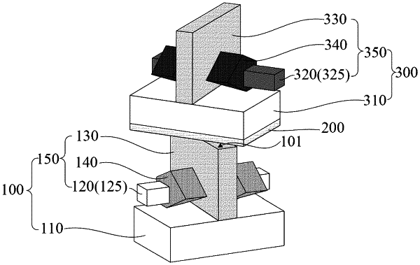
1. A forming method of a semiconductor structure, comprising:
forming a first device structure, comprising a first substrate and a first device formed on the first substrate, the first device comprising a first channel layer structure located on the first substrate, a first device gate structure extending across the first channel layer structure, and a first source-drain doping region located in the first channel layer structure on two sides of the first device gate structure, a surface, close to a top portion of the first device gate structure, in the first device structure being a front surface;
disposing a second substrate on the front surface of the first device structure;
forming a second channel layer structure on the second substrate after the second substrate is formed on the front surface of the first device structure, projections of the second channel layer structure and the first channel layer structure onto the first substrate intersecting non-orthogonally; and
forming a second device gate structure and a second source-drain doping region on the second substrate, the second device gate structure extending across the second channel layer structure, the second source-drain doping region being located in the second channel layer structure on two sides of the second device gate structure, the second source-drain doping region, the second device gate structure, and the second channel layer structure being configured to form a second device, the second device and the second substrate being configured to form a second device structure.
|