| CPC H01L 25/0657 (2013.01) [H01L 23/3128 (2013.01); H01L 24/08 (2013.01); H01L 2224/08146 (2013.01)] | 18 Claims |
|
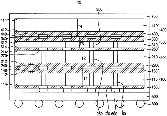
1. A semiconductor package, comprising:
a first semiconductor chip including a first substrate and a front insulation layer on a front surface of the first substrate and having a first bonding pad in an outer surface thereof;
a second semiconductor chip stacked on the first semiconductor chip, the second semiconductor chip including a second substrate, a second front insulation layer on a front surface of the second substrate and having a third bonding pad in an outer surface thereof, and a second backside insulation layer on a backside surface of the second substrate and having a fourth bonding pad in an outer surface thereof;
a third semiconductor chip stacked on the second semiconductor chip, the third semiconductor chip including a third substrate, a third front insulation layer on a front surface of the third substrate and having a fifth bonding pad in an outer surface thereof, and a through electrode penetrating through the third substrate to be electrically connected to the fifth bonding pad; and
a fourth semiconductor chip stacked on the third semiconductor chip, the fourth semiconductor chip including a fourth substrate and a fourth front insulation layer on a front surface of the fourth substrate and having a seventh bonding pad in an outer surface thereof,
wherein a backside of the third substrate is arranged to face the backside surface of the second substrate such that the third substrate and the second backside insulation layer are bonded directly to each other.
|