| CPC H01L 25/0655 (2013.01) [H01L 23/3192 (2013.01); H01L 23/49816 (2013.01); H01L 24/16 (2013.01); H01L 24/32 (2013.01); H01L 24/73 (2013.01); H01L 2224/16227 (2013.01); H01L 2224/32225 (2013.01); H01L 2224/73204 (2013.01); H01L 2924/3512 (2013.01)] | 20 Claims |
|
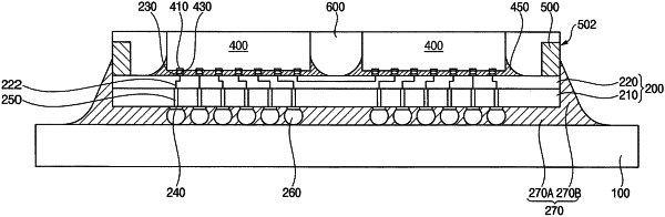
1. A semiconductor package, comprising:
a package substrate having a top surface and a bottom surface opposite to the top surface;
an interposer provided on the top surface of the package substrate, the interposer including a first side surface and a second side surface opposite to each other and a third side surface and a fourth second surface opposite to each other, the first side surface and the second side surface extending in a direction parallel with a first direction, the third side surface and the fourth second surface extending in a direction parallel with a second direction which is perpendicular to the first direction;
at least one first semiconductor device arranged in a middle region of the interposer;
at least four memory devices on the interposer and spaced apart from each other, two memory devices being arranged on a first side of the at least one first semiconductor device along the first side surface, another two memory devices being arranged on a second side, opposite to the first side, of the at least one first semiconductor device along the second side surface;
four dummy members on the interposer to cover four corner portions of the interposer respectively, four dummy members being arranged spaced apart from the respective memory devices, two dummy members being arranged adjacent to the first side surface, another two dummy members being arranged adjacent to the second side surface; and
a sealing member contacting the interposer and filling a space between the memory device and the dummy member so as to cover a first side surface of the memory device, a first side surface of the dummy member, and an upper surface of the dummy member,
wherein a second side surface, opposite to the first side surface, of the dummy member is uncovered by the sealing member,
wherein, when viewed in the first direction, two dummy members arranged adjacent to the first side surface partially overlap two memory devices arranged on the first side of the at least one first semiconductor device, and another two dummy members arranged adjacent to the second side surface overlap another two memory devices arranged on the second side of the at least one first semiconductor device, and
wherein, in a direction perpendicular to the top surface of the package substrate, a height of the dummy member is less than a height of the memory device.
|