| CPC H01L 25/0652 (2013.01) [H01L 21/561 (2013.01); H01L 21/6835 (2013.01); H01L 23/3128 (2013.01); H01L 23/5385 (2013.01); H01L 23/5386 (2013.01); H01L 23/544 (2013.01); H01L 24/32 (2013.01); H01L 24/83 (2013.01); H01L 25/50 (2013.01); H01L 2223/54426 (2013.01); H01L 2224/32225 (2013.01); H01L 2224/83005 (2013.01); H01L 2224/83896 (2013.01); H01L 2225/06541 (2013.01); H01L 2225/06586 (2013.01)] | 20 Claims |
|
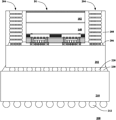
1. A structure, comprising:
stacked substrates;
a first semiconductor die laterally encapsulated by a first encapsulation portion;
a first bonding structure covering the first semiconductor die and the first encapsulation portion; and
a second semiconductor die comprising a second bonding structure electrically connected to the first bonding structure, the second semiconductor die and the second bonding structure being laterally encapsulated by a second encapsulation portion, the first bonding structure and the first semiconductor die being between the second semiconductor die and the stacked substrates, wherein the first encapsulation portion is spaced apart from the second encapsulation portion by the first bonding structure.
|