| CPC H01L 24/37 (2013.01) [H01L 24/40 (2013.01); H01L 2224/3701 (2013.01); H01L 2224/37005 (2013.01); H01L 2224/37013 (2013.01); H01L 2224/37149 (2013.01); H01L 2224/37171 (2013.01); H01L 2224/40229 (2013.01); H02M 1/0009 (2021.05)] | 18 Claims |
|
1. An electronic device, comprising:
a structured metallization layer comprising a plurality of contact pads that are electrically isolated from one another; and
a metal clip connected in a current shunt measurement arrangement with a semiconductor device,
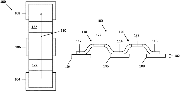
wherein the metal clip comprises first, second and third landing pads, a first bridge span connected between the first and second landing pads, and
second bridge span connected between the second and third landing pads,
wherein the first, second third landing pads are respectively thermally conductively attached to first, second and third contact pads from the structured metallization layer, and
wherein the second mounting pad is electrically floating.
|