| CPC H01L 24/05 (2013.01) [H01L 24/03 (2013.01); H01L 24/11 (2013.01); H01L 24/13 (2013.01); H01L 24/16 (2013.01); H01L 2224/02379 (2013.01); H01L 2224/03462 (2013.01); H01L 2224/03464 (2013.01); H01L 2224/03828 (2013.01); H01L 2224/03829 (2013.01); H01L 2224/0401 (2013.01); H01L 2224/05541 (2013.01); H01L 2224/05547 (2013.01); H01L 2224/05559 (2013.01); H01L 2224/05573 (2013.01); H01L 2224/05582 (2013.01); H01L 2224/05611 (2013.01); H01L 2224/05639 (2013.01); H01L 2224/11334 (2013.01); H01L 2224/11849 (2013.01); H01L 2224/13006 (2013.01); H01L 2224/13111 (2013.01); H01L 2224/13139 (2013.01); H01L 2224/16225 (2013.01); H01L 2924/3512 (2013.01)] | 14 Claims |
|
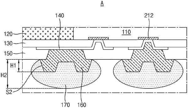
1. A wafer-level semiconductor package comprising:
a semiconductor chip including a first surface and a second surface, and including connection pads on the first surface;
a first passivation layer covering the first surface of the semiconductor chip, the first passivation layer including a plurality of first trenches exposing the connection pads;
redistribution layers in the first trenches and on the first passivation layer;
a second passivation layer on the redistribution layers, and the second passivation layer includes second trenches exposing the redistribution layers;
a plurality of UBM layers in the second trenches and on the second passivation and in contact with the redistribution layers, and the thickness of the UBM layer is approximately 25 to 35 μm; and
a plurality of solder bumps on the plurality of UBM layers, each of the plurality of solder bumps covering an outer surface of a corresponding one the plurality of UBM layers, and a thickness of each of the plurality of solder bumps is approximately 210 to 220 μm,
wherein at least one of the plurality of first trenches includes a portion of a corresponding one of the plurality UBM layers, and
at least one of a remainder of the plurality of first trenches includes a portion of the second passivation layer.
|