| CPC H01L 23/66 (2013.01) [G01S 7/028 (2021.05); G01S 13/931 (2013.01); H01L 23/49816 (2013.01); H03H 7/42 (2013.01); H01L 2223/6616 (2013.01); H01L 2223/6638 (2013.01); H01L 2223/6677 (2013.01); H01L 2223/6683 (2013.01)] | 17 Claims |
|
1. A packaged integrated circuit, comprising:
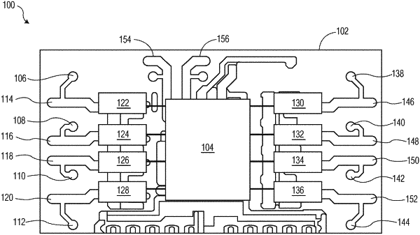
an integrated circuit (IC) die having a first external contact and a second external contact; a package substrate, wherein the IC die is attached to a first major surface of the package substrate, the package substrate including a balun in a first metal layer, wherein the balun is connected to the first and the second external contacts of the IC die and is connected to a first external contact of the package substrate, wherein the first and second external contacts of the IC die are configured to communicate a differential signal with the package substrate, and the first external contact of the package substrate is configured to communicate a single-ended signal corresponding to the differential signal.
|