| CPC H01L 23/562 (2013.01) [H01L 25/0652 (2013.01); H01L 25/0657 (2013.01); H01L 25/50 (2013.01); H01L 2225/0651 (2013.01); H01L 2225/06517 (2013.01); H01L 2225/06555 (2013.01); H01L 2225/06575 (2013.01); H01L 2225/06586 (2013.01)] | 13 Claims |
|
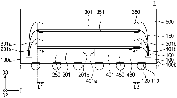
1. A semiconductor package comprising:
a substrate having a first side surface and a second side surface, which are opposite to each other;
a spacer on the substrate and insulated from the substrate;
a first semiconductor chip on the substrate to be horizontally spaced apart from the spacer and electrically connected to the substrate; and
a plurality of second semiconductor chips stacked in alignment on the spacer and the first semiconductor chip, such that all sidewalls of each of the plurality of second semiconductor chips are vertically aligned to corresponding sidewalls of the other second semiconductor chips;
wherein the spacer has an outer side surface, which is adjacent to the first side surface of the substrate, and an inner side surface, which is opposite to the outer side surface of the spacer;
wherein the first semiconductor chip has an outer side surface, which his adjacent to the second side surface of the substrate, and an inner side surface, which is opposite to the outer side surface of the first semiconductor chip;
wherein each of the plurality of second semiconductor chips has a third side surface, which is adjacent to the first side surface of the substrate, and a fourth side surface, which is opposite to the third side surface;
wherein the outer side surface of the spacer is farther from the first side surface of the substrate than the third side surface of the lowermost second semiconductor chips in a first direction parallel to a top surface of the substrate;
wherein the outer side surface of the first semiconductor chip is farther from the second side surface of the substrate than the fourth side surface of the lowermost second semiconductor chips in a direction antiparallel to the first direction; and
wherein a distance between the outer side surface of the spacer and the third side surface of the lowermost second semiconductor chip in the first direction is the same as the distance between the outer side surface of the first semiconductor chip and the fourth side surface of the lowermost second semiconductor chips in the first direction.
|