| CPC H01L 23/544 (2013.01) [H01L 23/18 (2013.01); H01L 23/295 (2013.01); H01L 25/0657 (2013.01); H01L 2223/5442 (2013.01); H01L 2225/0651 (2013.01); H01L 2225/06506 (2013.01); H01L 2225/06562 (2013.01)] | 19 Claims |
|
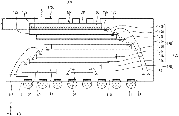
1. A semiconductor package, comprising:
a package substrate;
a chip structure including vertically stacked semiconductor chips disposed on the package substrate;
a spacer disposed on an uppermost semiconductor chip among the semiconductor chips;
an encapsulant covering at least part of the chip structure, and including an upper portion of the encapsulant covering at least part of the spacer; and
a marking pattern visually identifiable through an opening in the upper portion of the encapsulant selectively exposing portions of the spacer,
wherein the spacer includes at least one of monocrystalline silicon, polycrystalline silicon, amorphous silicon, monocrystalline gallium arsenide, polycrystalline gallium arsenide and amorphous gallium arsenide.
|