| CPC H01L 23/5386 (2013.01) [H01L 23/49816 (2013.01); H01L 23/5383 (2013.01); H01L 21/565 (2013.01)] | 19 Claims |
|
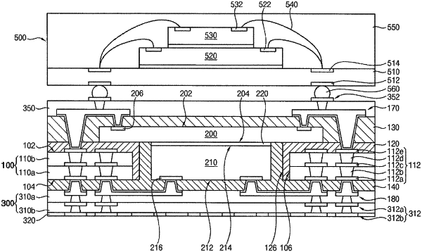
1. A semiconductor package, comprising:
a first molding member having an upper surface and a lower surface opposite to each other, the first molding member having a cavity that extends from the lower surface of the first molding member to a predetermined depth;
a first semiconductor chip on the upper surface of the first molding member;
a second semiconductor chip within the cavity, wherein a first surface of the second semiconductor chip on which second chip pads are formed is exposed from the lower surface of the first molding member;
a second molding member on the upper surface of the first molding member and covering the first semiconductor chip;
a third molding member on the lower surface of the first molding member, the third molding member filling the cavity and covering the first surface of the second semiconductor chip;
first redistribution wirings on the second molding member and electrically connected to first chip pads of the first semiconductor chip;
second redistribution wirings on the third molding member and electrically connected to the second chip pads of the second semiconductor chip;
a lower redistribution wiring layer on the third molding member and having lower redistribution wirings electrically connected to the second redistribution wirings, respectively; and
connection wirings electrically connecting the first redistribution wirings and the second redistribution wirings.
|