| CPC H01L 23/535 (2013.01) [H01L 23/4824 (2013.01); H01L 23/528 (2013.01); H01L 23/5222 (2013.01); H01L 23/53295 (2013.01); H01L 29/0649 (2013.01); H01L 29/41758 (2013.01); H01L 29/4238 (2013.01); H01L 29/66568 (2013.01); H01L 29/78 (2013.01); H01L 2924/0002 (2013.01)] | 40 Claims |
|
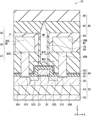
1. A field-effect transistor comprising:
a gate electrode;
a semiconductor layer having a source region and a drain region with the gate electrode in between;
contact plugs comprising a first conductive material, wherein a first contact plug of the contact plugs is provided on the source region, and wherein a second contact plug of the contact plugs is provided on the drain region;
first metals comprising a second conductive material that is different than the first conductive material, wherein one of the first metals is stacked on the first contact plug, and wherein a second one of the first metals is stacked on the second contact plug;
one or more insulating films provided (1) between the contact plugs along an in-plane direction of the semiconductor layer and (2) below bottom surfaces of the first metals along a stacking direction,
a first portion of the one or more insulating films provided between the contact plugs along the in-plane direction of the semiconductor layer and below the bottom surfaces of the first metals along the stacking direction, and the first portion of the one or more insulating films occupy a region between the first contact plug and a side surface of the gate electrode; and
a second portion of the one or more insulating films provided between the contact plugs along the in-plane direction of the semiconductor layer and above a first portion of a top surface of the gate electrode,
wherein a low-dielectric constant region provided in a region over a second portion of the top surface of the gate electrode, between the contact plugs along the in-plane direction of the semiconductor layer, and provided at least in a first region below the bottom surfaces of the first metals along the stacking direction, and
wherein the one or more insulating films at least include
a first insulating film at least extending along the side surface of the gate electrode,
a second insulating film, at least a portion of the first insulating film provided between the second insulating film and the gate electrode,
a third insulating film provided between the contact plugs along the in-plane direction, provided below the bottom surfaces of the first metals along the stacking direction, the third insulating film positioned outside a side section of the low-dielectric constant region, and
a fourth insulating film above a top surface of the third insulating film and between the side section of the low-dielectric constant region and the third insulating film.
|