| CPC H01L 23/53295 (2013.01) [H01L 21/31116 (2013.01); H01L 21/31144 (2013.01); H01L 21/76224 (2013.01); H01L 21/76804 (2013.01); H01L 21/76816 (2013.01); H01L 21/823418 (2013.01); H01L 21/823431 (2013.01); H01L 21/823437 (2013.01); H01L 21/823481 (2013.01); H01L 27/0886 (2013.01); H01L 29/0653 (2013.01); H01L 29/401 (2013.01); H01L 29/41791 (2013.01); H01L 29/6656 (2013.01); H01L 29/66545 (2013.01); H10B 10/12 (2023.02); H01L 29/086 (2013.01); H01L 29/0878 (2013.01)] | 15 Claims |
|
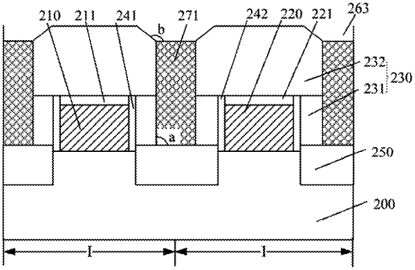
1. A semiconductor device, comprising:
a base substrate;
a first gate structure and doped source/drain layers on the base substrate, wherein the doped source/drain layers are on both sides of the first gate structure;
a dielectric layer on a surface of the base substrate, wherein the dielectric layer covers the doped source/drain layers, and the dielectric layer contains a first trench on the doped source/drain layer, wherein:
the first trench includes a first region filled by an insulation layer and a second region filled by a first conductive structure under the insulation layer;
a width of a top surface of the insulation layer in the first region is larger than a width of a bottom surface of the insulation layer in the first region;
a maximum width of the first conductive structure in the second region is smaller than the width of the bottom surface of the insulation layer in the first region;
a sidewall of the insulation layer in the first region is tilted; and
an angle between the sidewall of the insulation layer in the first region and a surface of the base substrate is a first angle including an obtuse angle;
a material of the insulation layer is different from a material of the dielectric layer; and
a second conductive structure is in the dielectric layer between insulation layers over adjacent doped source/drain layers, wherein the second conductive structure is connected to the first gate structure.
|