| CPC H01L 23/53238 (2013.01) [H01L 21/76804 (2013.01); H01L 21/76846 (2013.01); H01L 21/76877 (2013.01)] | 20 Claims |
|
1. A structure comprising:
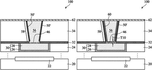
a first conductive feature in a first dielectric layer;
a second dielectric layer over the first dielectric layer; and a second conductive feature extending through the second dielectric layer to physically contact the first conductive feature, wherein the second conductive feature comprises:
a metal adhesion layer over and physically contacting the first conductive feature;
a barrier layer extending along sidewalls of the second dielectric layer, wherein the barrier layer and the metal adhesion layer are different materials; and
a conductive filling material extending over the metal adhesion layer and the barrier layer, wherein a portion of the conductive filling material extends laterally between an overlying portion of the barrier layer and an underlying portion of the metal adhesion layer, wherein a sidewall of the portion of the conductive filling material and a sidewall of the underlying portion of the metal adhesion layer are coplanar.
|