| CPC H01L 23/5223 (2013.01) | 20 Claims |
|
1. A substrate for semiconductor module, comprising:
a plurality of insulating layers provided in a sequentially stacked arrangement;
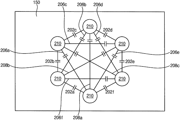
N signal lines transmitting N signals respectively, the N signal lines having N vias that at least partially penetrate through the plurality of insulating layers, the N vias being arranged in an N-sided polygon shape in a plan view; and
a capacitor element configured to provide capacitive coupling between the N signal lines, the capacitor element having a first coupling element configured to provide capacitive coupling between a first via and a second via adjacent to each other among the N vias and a second coupling element configured to provide capacitive coupling between a third via and a fourth via that are not adjacent to each other among the N vias,
wherein the first coupling element includes a first capacitive pattern extending from the first via toward the second via and a second capacitive pattern extending from the second via toward the first via, and the second coupling element includes a third capacitive pattern extending from the third via toward the fourth via and a fourth capacitive pattern extending from the fourth via toward the third via,
wherein the first capacitive pattern and the second capacitance pattern are provided in different insulating layers of the plurality of insulating layers, and a first region of the first capacitive pattern overlaps a second region of the second capacitance pattern in the plan view, and
wherein the third capacitive pattern and fourth capacitance pattern are provided in different insulating layers of the plurality of insulating layers, and a third region of the third capacitive pattern overlaps a fourth region of the fourth capacitance pattern in the plan view.
|
|
11. A substrate for semiconductor module, comprising:
a plurality of insulating layers sequentially arranged in a vertical direction;
N signal lines transmitting N signals respectively, the N signal lines having N vias that at least partially penetrate through the plurality of insulating layers and are arranged in an N-sided polygon shape in a plan view, N being a natural number greater than 3; and
at least one capacitor element having a first capacitive pattern extending from a first via of the N vias in a first horizontal direction and a second capacitance pattern extending from a second via of the N vias in a second horizontal direction parallel to the first horizontal direction, the first and second capacitive patterns configured to provide capacitive coupling between the first via and the second via,
wherein the first and second capacitive patterns provided in different insulating layers of the plurality of insulating layers, and the first and second capacitive patterns extend within the N-sided polygon shape in the plan view.
|
|
18. A semiconductor device, comprising:
a substrate having a plurality of layers stacked in a vertical direction; and
one or more memory packages provided on the substrate,
wherein the substrate comprises:
a plurality of signal lines penetrating the substrate in the vertical direction, the plurality of signal lines having a plurality of vias arranged in a circumferential direction at predetermined intervals around a center of the vias; and
a first coupling element and a second coupling element configured to provide capacitive coupling between the signal lines, the first coupling element configured to provide capacitive coupling between first and second vias that are sequentially arranged to be adjacent with each other in the circumferential direction, the second coupling element configured to provide capacitive coupling between third and fourth vias that are not sequentially arranged each other in the circumferential direction,
wherein the first coupling element includes a first capacitive pattern extending from the first via toward the second via and a second capacitive pattern extending from the second via toward the first via,
wherein the second coupling element includes a third capacitive pattern extending from the third via toward the fourth via and a fourth capacitive pattern extending from the fourth via toward the third via,
wherein the first capacitive pattern and second capacitive pattern are provided in different layers of the plurality of layers and a first region of the first capacitive pattern overlaps a second region of the second capacitance pattern in the vertical direction, and
wherein the third capacitive pattern and fourth capacitive pattern are provided in different layers of the plurality of layers and a third region of the third capacitive pattern overlaps a fourth region of the fourth capacitance pattern in the vertical direction.
|