| CPC H01L 23/5223 (2013.01) [H01L 21/76843 (2013.01); H01L 23/528 (2013.01); H01L 28/60 (2013.01); H01L 21/76898 (2013.01); H01L 23/5226 (2013.01); H01L 24/80 (2013.01); H01L 25/0657 (2013.01)] | 10 Claims |
|
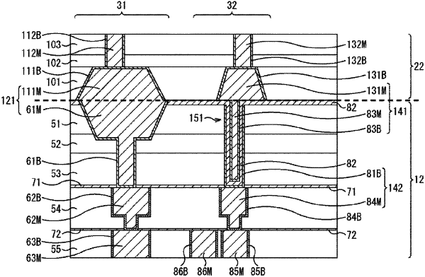
1. A semiconductor device, comprising:
a first semiconductor substrate;
a first multilayer wiring layer formed on the first semiconductor substrate, wherein the first multilayer wiring layer includes a plurality of insulating layers;
a second semiconductor substrate;
a second multilayer wiring layer formed on the second semiconductor substrate, wherein the first multilayer wiring layer is bonded to the second multilayer wiring layer at a junction plane; and
a capacitive element, wherein the capacitive element includes a first electrode at least partially formed in first and second insulating layers of the first multilayer wiring layer, and a second electrode at least partially formed in the first and second insulating layers of the first multilayer wiring layer.
|