| CPC H01L 23/49838 (2013.01) [H01L 21/4857 (2013.01); H01L 23/49816 (2013.01); H01L 23/49822 (2013.01); H01L 23/49827 (2013.01); H05K 1/11 (2013.01); H05K 1/111 (2013.01); H05K 1/182 (2013.01); H01L 23/3128 (2013.01); H01L 23/3135 (2013.01); H01L 23/5383 (2013.01); H01L 24/16 (2013.01); H01L 24/48 (2013.01); H01L 25/0657 (2013.01); H01L 2224/16227 (2013.01); H01L 2224/48229 (2013.01); H05K 1/0284 (2013.01); H05K 1/0298 (2013.01); H05K 1/0306 (2013.01); H05K 1/0313 (2013.01); H05K 1/115 (2013.01); H05K 1/18 (2013.01); H05K 1/181 (2013.01); H05K 2201/10378 (2013.01)] | 20 Claims |
|
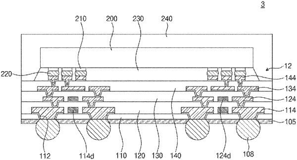
1. A connection structure comprising:
a first passivation layer comprises an opening;
a first conductive pattern that penetrates the first passivation layer and protrudes upwardly from the first passivation layer;
a second passivation layer on the first passivation layer and covering the first conductive pattern;
a second conductive pattern on the second passivation layer and electrically connected to the first conductive pattern;
a third passivation layer on the second passivation layer and covering the second conductive pattern;
a third conductive pattern on the third passivation layer and electrically connected to the second conductive pattern; and
an external terminal in the opening and electrically connected to the first conductive pattern,
wherein the first conductive pattern is thicker than the second conductive pattern, and the second conductive pattern is thicker than the third conductive pattern,
wherein a width of the first conductive pattern is greater than a width of the second conductive pattern, and the width of the second conductive pattern is equal to or greater than a width of the third conductive pattern, and
wherein a pitch between patterns of the first conductive pattern is greater than a pitch between patterns of the second conductive pattern, and the pitch between the patterns of the second conductive pattern is equal to or greater than a pitch between patterns of the third conductive pattern.
|