| CPC H01L 23/49838 (2013.01) [H01L 23/5389 (2013.01); H01L 24/06 (2013.01); H01L 24/14 (2013.01); H01L 23/3128 (2013.01); H01L 23/49816 (2013.01); H01L 2224/0401 (2013.01); H01L 2224/18 (2013.01); H01L 2924/1431 (2013.01); H01L 2924/1433 (2013.01); H01L 2924/3511 (2013.01)] | 20 Claims |

|
1. A fan-out semiconductor package comprising:
a semiconductor chip comprising:
an active surface comprising a connection pad disposed on the active surface of the semiconductor chip; and
an inactive surface opposing the active surface;
an encapsulant encapsulating at least a portion of the inactive surface of the semiconductor chip; and
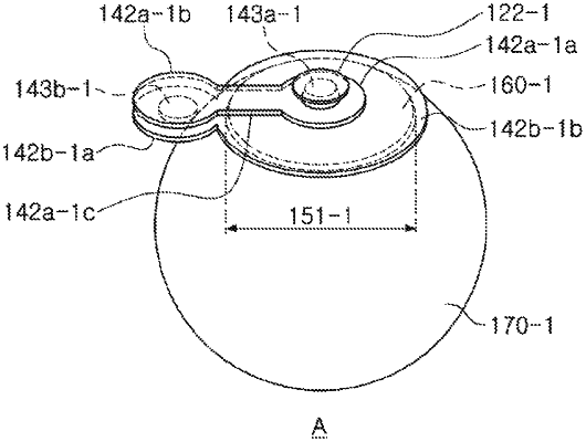
an interconnection member comprising a first conductive structure and a second conductive structure, a first surface of the interconnection member being disposed on the active surface of the semiconductor chip,
wherein the first conductive structure comprises:
a first via adjacent to the first surface of the interconnection member;
a first via pad extended from the first via in a direction parallel to the first surface;
a second via connected to the first via pad; and
a second via pad extended from the second via in the direction parallel to the first surface,
wherein the second conductive structure comprises:
a third via adjacent to the connection pad; and
a third via pad connected to the third via,
wherein the first via comprises a first central axis and the second via comprises a second central axis, the first central axis and the second central axis being displaced in the direction parallel to the first surface,
wherein the first conductive structure is disposed farther from a central axis of the semiconductor chip than the second conductive structure.
|