| CPC H01L 23/49827 (2013.01) [H01L 21/486 (2013.01); H01L 25/0753 (2013.01); H01L 25/167 (2013.01); H01L 33/62 (2013.01); H01L 33/641 (2013.01); H01L 33/642 (2013.01); H01L 23/15 (2013.01); H01L 23/373 (2013.01); H01L 23/3731 (2013.01); H01L 23/3732 (2013.01); H01L 23/3733 (2013.01); H01L 23/3736 (2013.01); H01L 23/3738 (2013.01); H01L 2224/48091 (2013.01); H01L 2933/0066 (2013.01); H01L 2933/0075 (2013.01)] | 7 Claims |
|
1. A method for producing a carrier comprising the steps:
A) providing an electrically conductive first auxiliary carrier;
B) arranging at least one thermal connection element on the first auxiliary carrier;
C) arranging at least one through-connection on the first auxiliary carrier;
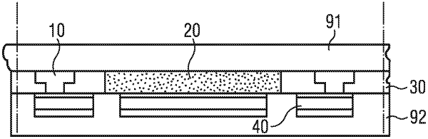
D) applying a base material to the first auxiliary carrier, wherein the base material completely surrounds the through-connection and the thermal connection element in lateral directions;
E) applying contact structures on a side of the thermal connection element and the through-connection facing away from the first auxiliary carrier;
F) arranging a second auxiliary carrier on a side of the contact structures facing away from the first auxiliary carrier;
G) removing the first auxiliary carrier;
H) applying a metallization to a side of the thermal connection element and/or the through-connection facing away from the second auxiliary carrier; and
I) removing the second auxiliary carrier;
wherein
after step I) a substrate is arranged on a side of the metallization facing away from the base material, wherein the substrate comprises at least one conductor track and at least one heat sink;
the metallization, which is arranged in the region of the through-connection, is brought into direct contact with the conductor track; and
the metallization, which is arranged in the region of the thermal connection element, is brought into direct contact with the heat sink.
|