| CPC H01L 23/49565 (2013.01) [H01L 21/4825 (2013.01); H01L 21/4828 (2013.01); H01L 21/565 (2013.01); H01L 21/78 (2013.01); H01L 23/49503 (2013.01); H01L 23/49513 (2013.01); H01L 23/49548 (2013.01); H01L 23/49562 (2013.01); H01L 2224/16245 (2013.01); H01L 2224/97 (2013.01); H01L 2924/181 (2013.01)] | 17 Claims |
|
1. A semiconductor device, comprising:
a semiconductor die;
an encapsulant deposited over the semiconductor die; and
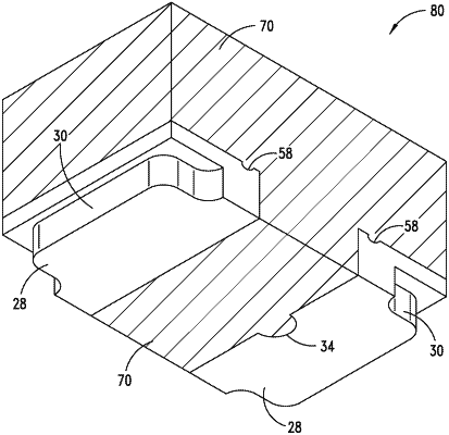
a plurality of contacts exposed from the encapsulant, wherein each of the plurality of contacts includes a half-etched portion forming a side surface that extends for an entire length or width of the encapsulant, wherein the side surface includes a convex U-shaped curve, and wherein the side surface includes a solder wettable layer formed over the side surface including on the convex U-shaped curve.
|