| CPC H01L 23/49531 (2013.01) [H01L 23/49575 (2013.01); H01L 23/49816 (2013.01); H01L 23/5386 (2013.01); H01L 24/32 (2013.01); H01L 24/48 (2013.01); H01L 25/0657 (2013.01); H01L 2224/32245 (2013.01); H01L 2224/48091 (2013.01); H01L 2224/48145 (2013.01); H01L 2924/186 (2013.01)] | 20 Claims |
|
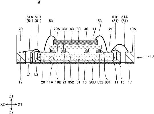
1. A semiconductor device comprising:
a lead frame having a first principal surface which includes a recess, and a second principal surface opposite to the first principal surface;
a relay board, disposed in the recess, and having a third principal surface, and a fourth principal surface opposite to the third principal surface and bonded to a surface of the lead frame forming a bottom of the recess;
a first semiconductor chip disposed on the third principal surface;
a first conductive material electrically connecting the lead frame and the relay board; and
a second conductive material electrically connecting the relay board and the first semiconductor chip,
wherein a distance between the second principal surface and the third principal surface is less than or equal to a distance between the second principal surface and the first principal surface.
|