| CPC H01L 23/49503 (2013.01) [H01L 23/4952 (2013.01); H01L 23/49575 (2013.01); H01L 23/49816 (2013.01)] | 19 Claims |
|
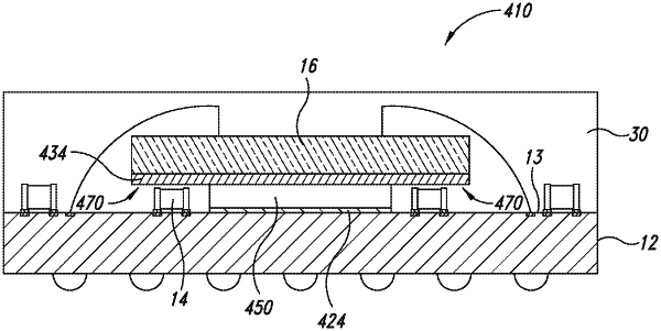
7. A method, comprising:
coupling a first electrical discrete component to a surface of a substrate;
coupling a non-active silicon spacer devoid of electrical circuitry to the surface of the substrate with a first adhesive layer; and
coupling a central region of an active die having a width greater than a width of the non-active silicon spacer to the non-active silicon spacer with a second adhesive layer, the coupling the central region of the active die to the non-active silicon spacer including:
covering the non-active silicon spacer with a central portion of the active die; and
overlapping the first electrical discrete component with a peripheral overhang portion of the active die extending outward from the central portion of the active die; and
overlapping the first electrical discrete component with the second adhesive layer, and the second adhesive layer being spaced apart from the first electrical discrete component.
|