| CPC H01L 23/481 (2013.01) [H01L 24/05 (2013.01); H01L 24/08 (2013.01); H01L 24/80 (2013.01); H01L 25/0657 (2013.01); H10B 12/0335 (2023.02); H10B 12/315 (2023.02); H10B 12/50 (2023.02); H01L 2224/05147 (2013.01); H01L 2224/08146 (2013.01); H01L 2224/80896 (2013.01); H01L 2225/06524 (2013.01); H01L 2225/06544 (2013.01); H01L 2924/1431 (2013.01); H01L 2924/1436 (2013.01)] | 27 Claims |
|
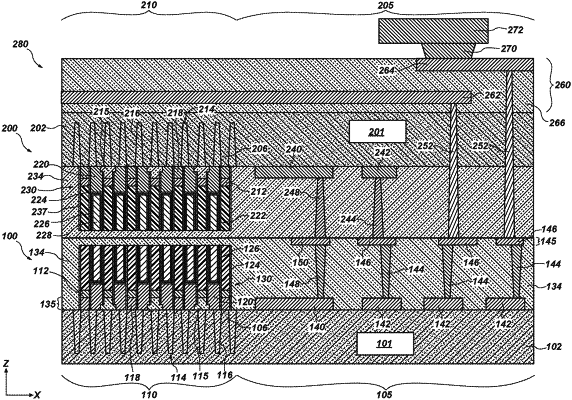
1. A microelectronic device, comprising:
a first microelectronic device structure comprising:
a first memory array region comprising memory cells, each of the memory cells comprising:
an access device; and
a charge storage device operably coupled to the access device; and
a first base structure comprising first control logic devices configured to effectuate one or more control operations of the memory cells of the first memory array region, each access device of the first memory array region located within the first base structure; and
a second microelectronic device structure attached to the first microelectronic device, the second microelectronic device structure comprising:
a second memory array region comprising additional memory cells, each of the additional memory cells comprising:
an additional access device; and
an additional charge storage device operably coupled to the additional access device; and
a second base structure comprising second control logic devices configured to effectuate one or more control operations of the additional memory cells of the second memory array region.
|