| CPC H01L 23/481 (2013.01) [H01L 23/3171 (2013.01); H01L 23/49816 (2013.01); H01L 23/49822 (2013.01); H01L 23/49833 (2013.01); H01L 23/49838 (2013.01); H01L 23/5385 (2013.01); H01L 23/5386 (2013.01); H01L 24/08 (2013.01); H01L 24/16 (2013.01); H01L 25/0655 (2013.01); H01L 25/0657 (2013.01); H01L 2224/0214 (2013.01); H01L 2224/0215 (2013.01); H01L 2224/02125 (2013.01); H01L 2224/08059 (2013.01); H01L 2224/16146 (2013.01); H01L 2224/16148 (2013.01); H01L 2224/16237 (2013.01); H01L 2225/06513 (2013.01); H01L 2225/06517 (2013.01); H01L 2225/06544 (2013.01); H01L 2225/06548 (2013.01); H01L 2924/1431 (2013.01); H01L 2924/1434 (2013.01); H01L 2924/3512 (2013.01)] | 20 Claims |
|
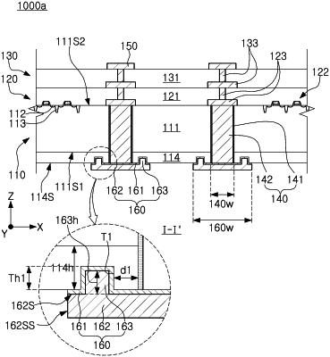
1. A semiconductor package comprising:
a plurality of semiconductor chips electrically connected to each other and stacked in a first direction,
wherein at least one of the plurality of semiconductor chips includes
a semiconductor substrate including a semiconductor layer having a first surface and a second surface that are opposite each other,
a passivation layer on the first surface and having a third surface that is opposite the first surface,
a circuit structure on the second surface,
a frontside pad on the circuit structure,
a backside pad on the third surface, and
a through-via in the semiconductor substrate and extending between the second surface and the third surface to be electrically connected to the backside pad and the frontside pad,
wherein the backside pad includes an electrode pad portion, on the third surface, and a dam structure protruding into the passivation layer toward the first surface of the semiconductor layer on one side of the electrode pad portion and surrounding a side surface of the through-via,
wherein the dam structure is spaced apart from the side surface of the through-via, and
wherein a height of the dam structure in the first direction into the passivation layer is less than a thickness of the passivation layer.
|