US 11,810,831 B2
Integrated circuit package and method of forming same
Chen-Hua Yu, Hsinchu (TW); Chih-Wei Wu, Zhuangwei Township (TW); Ying-Ching Shih, Hsinchu (TW); and Szu-Wei Lu, Hsinchu (TW)
Assigned to TAIWAN SEMICONDUCTOR MANUFACTURING COMPANY, LTD., Hsinchu (TW)
Filed by Taiwan Semiconductor Manufacturing Co., Ltd., Hsinchu (TW)
Filed on Jul. 25, 2022, as Appl. No. 17/872,488.
Application 17/872,488 is a continuation of application No. 17/068,064, filed on Oct. 12, 2020, granted, now 11,424,173.
Application 17/068,064 is a continuation of application No. 16/697,898, filed on Nov. 27, 2019, granted, now 10,804,178, issued on Oct. 13, 2020.
Application 16/697,898 is a continuation of application No. 16/176,008, filed on Oct. 31, 2018, granted, now 10,529,637, issued on Jan. 7, 2020.
Prior Publication US 2022/0359329 A1, Nov. 10, 2022
Int. Cl. H01L 23/31 (2006.01); H01L 25/065 (2023.01); H01L 21/56 (2006.01); H01L 25/00 (2006.01); H01L 23/18 (2006.01); H01L 21/822 (2006.01); H01L 25/11 (2006.01)
CPC H01L 23/3135 (2013.01) [H01L 21/56 (2013.01); H01L 23/18 (2013.01); H01L 25/0657 (2013.01); H01L 25/50 (2013.01); H01L 21/563 (2013.01); H01L 21/568 (2013.01); H01L 21/8221 (2013.01); H01L 25/117 (2013.01); H01L 2225/06513 (2013.01)] 20 Claims
OG exemplary drawing
 
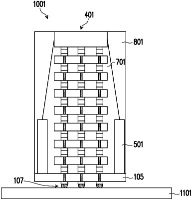
1. A package comprising:
a substrate;
a dam structure attached to the substrate;
a die stack attached to the substrate, the die stack being between portions of the dam structure, a topmost surface of the die stack being above a topmost surface of the dam structure, a topmost surface of at least one die of the die stack being below the topmost surface of the dam structure; and
a first encapsulant surrounding the die stack and extending between the dam structure and the die stack; and
a second encapsulant over the first encapsulant, wherein the second encapsulant extends along sidewalls of a topmost die of the die stack.