| CPC H01L 21/823842 (2013.01) [H01L 21/32134 (2013.01)] | 19 Claims |
|
1. A method for fabricating a semiconductor device, the method comprising:
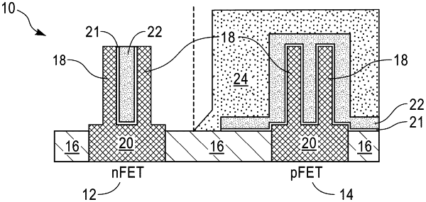
conformally depositing a work function metal over channel structures provided in an nFET region and a pFET region of a semiconductor device;
depositing and patterning an organic planarizing layer to block the channel structures in a selected one of the nFET region and the pFET region;
removing a nominal thickness of the work function metal from the other one of the nFET and pFET region, wherein removing the nominal thickness laterally removes a portion of the work function metal to form an undercut in the organic planarizing layer;
reflowing the organic planarizing layer to fill the undercut and completely cover the work function metal underlying the organic planarizing layer by irradiating the organic planarizing layer;
irradiating, after reflowing the organic planarizing layer, the organic planarizing layer to re-crosslink the organic planarization layer; and
fully removing a remaining portion of work function metal from the other one of the nFET region and the pFET region, wherein fully removing the remaining work function metal does not remove any additional amount of the work function metal underlying the organic planarizing layer.
|