| CPC H01L 21/784 (2013.01) [H01L 23/544 (2013.01); H01L 2223/5446 (2013.01)] | 16 Claims |
|
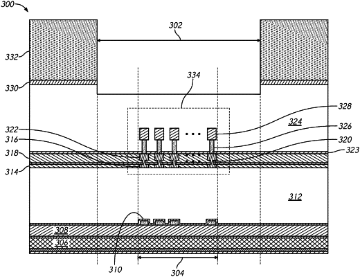
1. An apparatus comprising:
a first chip and a second chip;
a scribe region between the first chip and the second chip; and
a crack guide region in the scribe region, the crack guide region including a dicing line along which the first chip and the second chip are to be divided;
wherein the apparatus includes, in the crack guide region, a first set of lines in a first insulating layer, a set of vias in the first insulating layer, a second set of lines in a second insulating layer, and a third set of lines in a third insulating layer,
wherein a first end of each via in the set of vias adjoins a first line of the first set of lines and a second end of each via in the set of vias adjoins a second line of the second set of lines, and
wherein no vias adjoin the third set of lines.
|