| CPC H01L 21/7682 (2013.01) [H01L 23/5329 (2013.01); H01L 21/764 (2013.01); H01L 23/528 (2013.01); H01L 23/5283 (2013.01); H01L 23/53295 (2013.01)] | 20 Claims |
|
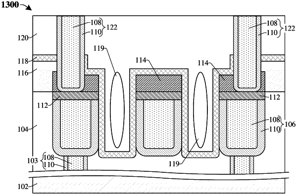
1. A semiconductor structure comprising:
a conductive wire disposed within a first dielectric structure;
an etch stop layer overlying the first dielectric structure;
a dielectric capping layer disposed between an upper surface of the conductive wire and the etch stop layer; and
an upper dielectric layer disposed along sidewalls of the conductive wire and an upper surface of the etch stop layer, wherein the upper dielectric layer comprises a lateral segment, a first vertical segment, and a second vertical segment, wherein the lateral segment continuously extends from the first vertical segment to the second vertical segment, wherein the lateral segment contacts an upper surface of the dielectric capping layer, and wherein the first vertical segment contacts a first sidewall of the dielectric capping layer and the second vertical segment contacts a second sidewall of the dielectric capping layer.
|