| CPC H01L 21/76802 (2013.01) [H01L 21/76877 (2013.01); H10B 41/27 (2023.02); H10B 43/27 (2023.02)] | 20 Claims |

|
1. A vertical semiconductor device comprising:
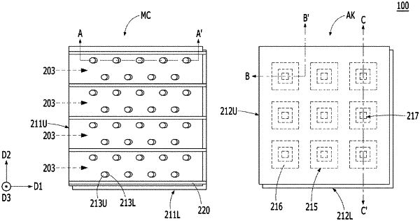
a substrate including a memory cell region and an alignment key region;
a memory cell stack in which dielectric layers and gate electrodes are alternately stacked in the memory cell region;
a dummy stack formed in the alignment key region;
a lower channel structure that penetrates a lower portion of the memory cell stack;
an upper channel structure that penetrates an upper portion of the memory cell stack and is located on the lower channel structure;
a lower stepped alignment key having a trench shape and disposed in a lower portion of the dummy stack; and
an upper stepped alignment key disposed in an upper portion of the dummy stack and caused by the lower stepped alignment key.
|
|
11. A semiconductor device comprising:
a substrate including an alignment key region;
a dummy stack formed in the alignment key region;
a lower stepped alignment key having a trench shape and disposed in a lower portion of the dummy stack; and
an upper stepped alignment key disposed in an upper portion of the dummy stack and caused by the lower stepped alignment key.
|