| CPC H01L 21/67092 (2013.01) [H01L 21/67253 (2013.01); H01L 21/67271 (2013.01); H01L 21/67288 (2013.01); H01L 21/681 (2013.01); H01L 21/6831 (2013.01); H01L 21/68714 (2013.01); H01L 22/20 (2013.01); H01L 22/12 (2013.01)] | 34 Claims |
|
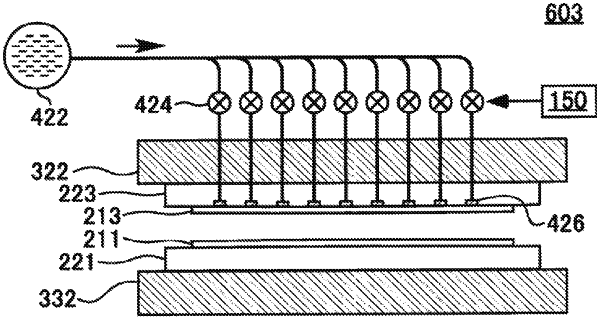
1. A stacked substrate manufacturing method by bonding a first substrate and a second substrate, the stacked substrate manufacturing method comprising:
obtaining information about curving of the first substrate; and
at least one of:
(i) estimating, based on the information about curving, an amount of distortion occurring in the first substrate while a contact region formed between the first substrate and the second substrate is spreading; and
(ii) calculating, based on the information about curving, an amount of misalignment between the first substrate and the second substrate, the misalignment occurring while the contact region formed between the first substrate and the second is spreading.
|