| CPC H01L 21/31116 (2013.01) [H01J 37/32449 (2013.01); H01J 2237/334 (2013.01); H01L 21/76802 (2013.01)] | 15 Claims |
|
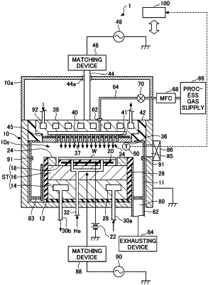
1. An etching method comprising:
mounting a substrate on a stage in a processing chamber, the substrate including a laminate film that includes at least (i) a silicon-containing insulating layer, (ii) an underlying layer disposed in the silicon-containing insulating layer, and (iii) a mask layer disposed in an upper layer of the silicon-containing insulating layer;
supplying process gas to the processing chamber, the process gas including at least one of fluorocarbon gas or hydrofluorocarbon gas;
selecting, based on a combination of material of the silicon-containing insulating layer and material of the underlying layer, a surface temperature range of at least one member of a first member or a second member in the processing chamber, the first member facing the substrate, and the second member being provided to encircle the substrate;
adjusting a surface temperature of the one member to be within the selected surface temperature range; and
forming a plasma in the processing chamber to which the process gas is supplied, thereby etching the silicon-containing insulating layer.
|