| CPC H01L 21/3088 (2013.01) | 12 Claims |
|
1. A method for forming a semiconductor structure, comprising:
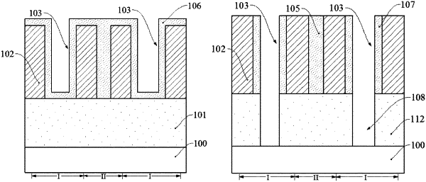
providing a base, wherein the base comprises first regions and a second region located between the first regions;
forming a pattern definition layer on the base;
forming discrete mask layers on the pattern definition layer, the mask layers and the base defining openings, where the openings of the first regions serve as first openings, and an opening of the second region serves as a second opening;
forming a filling layer in the second opening; and
etching, using the mask layers and the filling layer as masks, the pattern definition layer exposed from the first openings, to form target patterns.
|