| CPC H01L 21/02389 (2013.01) [H01L 21/0254 (2013.01); H01L 21/02694 (2013.01); H01L 21/30625 (2013.01); H01L 29/2003 (2013.01); H01L 29/401 (2013.01); H01L 29/454 (2013.01)] | 8 Claims |
|
1. A gallium nitride semiconductor device comprising:
a chip formation substrate made of gallium nitride and having one surface and an other surface opposite to the one surface;
a one surface side element component disposed on the one surface and providing a component of an one surface side of a semiconductor element; and
a metal film constituting a back surface electrode in contact with the other surface, wherein:
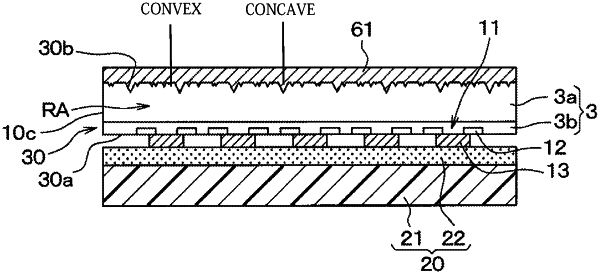
the other surface has an irregularity provided by
a plurality of convex portions with a trapezoidal cross section and
a plurality of concave portions located between the convex portions;
an upper base surface of the trapezoidal cross section in each of the plurality of convex portions is opposed to the one surface; and
a maximum depth of some of the concave portions vary.
|