| CPC H01L 33/60 (2013.01) [H01L 33/38 (2013.01); H01L 33/486 (2013.01); H01L 33/50 (2013.01); H01L 33/52 (2013.01); H01L 24/45 (2013.01); H01L 24/73 (2013.01); H01L 33/62 (2013.01); H01L 2224/16245 (2013.01); H01L 2224/32245 (2013.01); H01L 2224/45144 (2013.01); H01L 2224/48091 (2013.01); H01L 2224/48247 (2013.01); H01L 2224/48465 (2013.01); H01L 2224/73265 (2013.01); H01L 2924/181 (2013.01); H01L 2924/1815 (2013.01)] | 21 Claims |
|
1. An optical semiconductor element mounting package having a recessed part that serves as an optical semiconductor element mounting region, wherein the package is formed by integrating:
a resin molding composed of a thermosetting light-reflecting resin composition, which forms at least the side faces of the recessed part; and
at least a pair of positive and negative lead electrodes disposed opposite to each other so as to form part of the bottom face of the recessed part, wherein there is no gap at a joint face between the resin molding and the lead electrodes, and an outer surface of the resin molding and an outer surface of the at least one of the lead electrodes are planar at an outer surface of the package,
wherein each one of the lead electrodes includes a metal film on a surface of the lead electrodes so as to form part of the bottom face of the recessed part, and
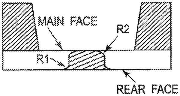
wherein the positive lead electrode has a first inner end, the negative lead electrode has a second inner end opposite to the first inner end of the positive lead electrode, and at least one side face of the first inner end and the second inner end is curved, and wherein the positive lead electrode and the negative lead electrode are not bent.
|