| CPC H01L 23/535 (2013.01) [H01L 23/5226 (2013.01); H01L 23/5283 (2013.01); H10B 41/27 (2023.02); H10B 41/41 (2023.02); H10B 43/27 (2023.02); H10B 43/40 (2023.02)] | 20 Claims |
|
1. A semiconductor device, comprising:
a lower structure;
a stack structure on the lower structure, the stack structure being in a memory cell array region and extending into a connection region, and the stack structure including interlayer insulating layers and horizontal layers alternately stacked in the memory cell array region and extending into the connection region;
an upper insulating layer on the stack structure;
gate contact plugs in the connection region; and
a memory vertical structure penetrating through the stack structure in the memory cell array region,
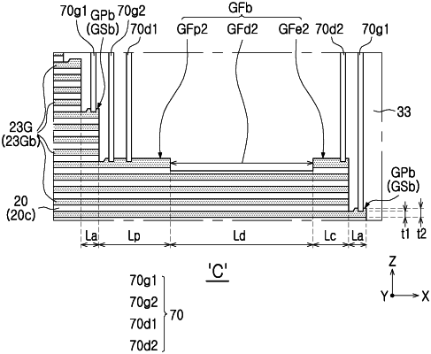
wherein, in the connection region, a first cross-sectional structure of the stack structure includes a first gate staircase region and a first gate flat region adjacent to the first gate staircase region,
wherein the first gate staircase region includes first gate pads lowering in a first horizontal direction by a first height therebetween, the first horizontal direction being oriented from the memory cell array region toward the connection region,
wherein the first gate flat region includes a first gate flat pad region, a first gate flat edge region, and a first gate flat dummy region between the first gate flat pad region and the first gate flat edge region, topmost surfaces of the first gate flat pad region and the first gate flat edge region being at a same level, and
wherein the gate contact plugs include first gate contact plugs in contact with the first gate pads on the first gate pads, flat contact plugs in contact with the first gate flat pad region on the first gate flat pad region, and an edge flat contact plug in contact with the first gate flat edge region on the first gate flat edge region.
|