| CPC H01L 23/3735 (2013.01) [H01L 21/52 (2013.01); H01L 23/3107 (2013.01); H01L 23/3114 (2013.01); H01L 23/3121 (2013.01); H01L 23/3135 (2013.01); H01L 23/4334 (2013.01); H01L 23/49822 (2013.01); H01L 24/20 (2013.01); H01L 25/0657 (2013.01); H01L 25/072 (2013.01); H01L 25/50 (2013.01); H01L 29/7393 (2013.01); H01L 29/861 (2013.01); H01L 2225/06589 (2013.01)] | 18 Claims |
|
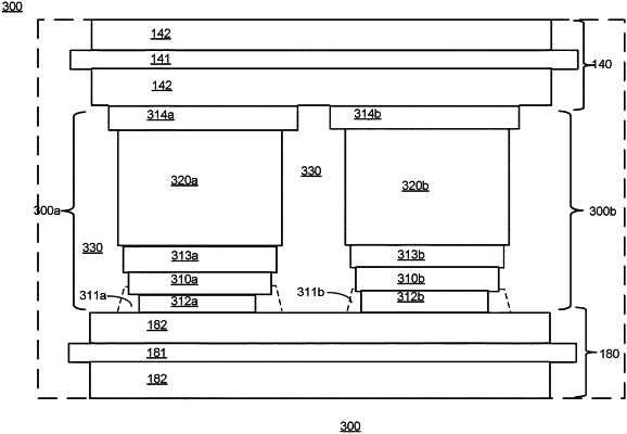
1. A method, comprising:
disposing a semiconductor die and a conductive spacer between a first high voltage isolation carrier and a second high voltage isolation carrier, the semiconductor die being thermally coupled to the conductive spacer, the semiconductor die being electrically coupled to the first high voltage isolation carrier by a coupling layer;
disposing a first molding material in contact with the coupling layer in a space between the semiconductor die and the first high voltage isolation carrier, the first molding material being an electrically isolating material; and
encapsulating the first molding material and the conductive spacer with a second molding material, the second molding material being an electrically isolating material.
|