| CPC H01J 31/26 (2013.01) [H01J 29/04 (2013.01); H01J 29/085 (2013.01)] | 15 Claims |
|
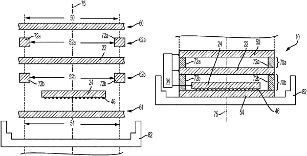
1. An image intensifier apparatus, comprising:
a photocathode wafer comprising a plurality of photocathode regions;
an interconnect wafer comprising a plurality of electrically separate sets of conductive traces formed in or upon the interconnect wafer;
a plurality of imager anodes integrated among or bonded to corresponding electrically separate sets of conductive traces;
an insulative spacer wafer with openings therein aligned over the imager anodes and between the interconnect wafer and the photocathode wafer; and
gaps within each space of a plurality of spaces formed between each imager anode of the plurality of imager anodes and each of the respective plurality of photocathodes through which the plurality of spaces are simultaneously evacuated to concurrently form a plurality of image intensifiers thereafter diced to form the image intensifier apparatus.
|