| CPC H01F 27/292 (2013.01) [H01F 17/0013 (2013.01); H01F 17/04 (2013.01); H01F 27/2804 (2013.01); H01F 41/041 (2013.01); H05K 1/181 (2013.01); H01F 2017/048 (2013.01)] | 8 Claims |

|
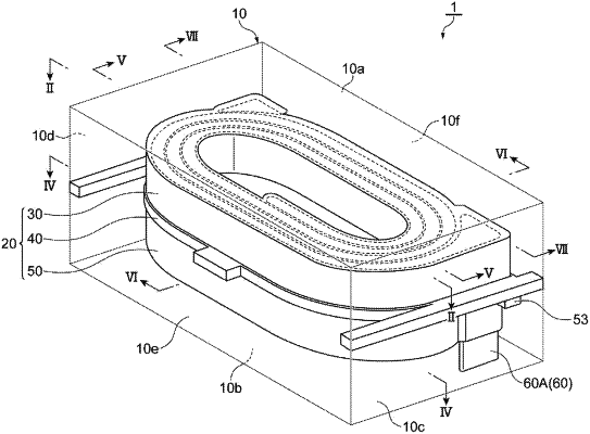
1. A coil component comprising:
an element body including a magnetic material and having an upper surface and a lower surface parallel to each other;
a substrate disposed in the element body and extending in parallel to the upper and lower surfaces;
a first coil body disposed in the element body, formed on an upper surface of the substrate, and having a first planar coil having a first connection end portion, a first extracting end portion, and a first turn portion interconnecting the first connection end portion and the first extracting end portion and a first insulator covering the first planar coil in the same layer as a layer where the first planar coil is formed;
a second coil body disposed in the element body, formed on a lower surface of the substrate, and having a second planar coil having a second connection end portion connected to the first connection end portion of the first planar coil via the substrate, a second extracting end portion, and a second turn portion interconnecting the second connection end portion and the second extracting end portion and a second insulator covering the second planar coil in the same layer as a layer where the second planar coil is formed;
a pair of terminal electrodes provided on the lower surface of the element body; and
a pair of bump electrodes extending along a thickness direction of the substrate and respectively interconnecting the first and second extracting end portions of the first and second planar coils and the pair of terminal electrodes, wherein
each of the pair of bump electrodes is positioned in a corner portion of a rectangular region including the first coil body and the second coil body when viewed from the thickness direction of the substrate, and
at least an end portion of one of the pair of bump electrodes on the substrate side overlaps neither the first turn portion of the first planar coil nor the second turn portion of the second planar coil in the thickness direction of the substrate and at least an end portion of the other bump electrode on the substrate side overlaps neither the first turn portion of the first planar coil nor the second turn portion of the second planar coil in the thickness direction of the substrate.
|