| CPC G11C 7/1063 (2013.01) [G11C 7/109 (2013.01); G11C 7/1015 (2013.01); H03K 19/20 (2013.01)] | 44 Claims |
|
1. A memory module, comprising:
a memory array of storage transistors; and
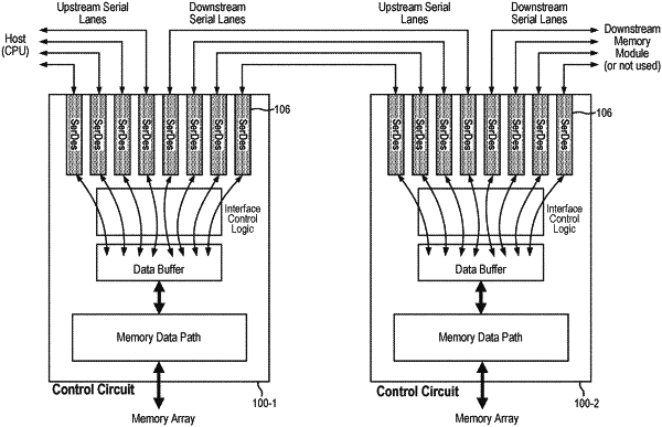
a control circuit for accessing and operating the memory array, the control circuit comprising a memory interface circuit, the memory interface circuit comprising a plurality of transceivers, each transceiver to be connected to a respective serial data lane, the memory interface circuit configuring a first subset of the transceivers for upstream connections for connecting through one or more serial data lanes to a host processor or connecting to transceivers of an upstream memory module and a second subset of the transceivers for downstream connections for connecting through one or more serial data lanes to transceivers of a downstream memory module,
wherein the control circuit receives a data packet from the host processor or the upstream memory module and inspects the memory address associated with the data packet, and in response to the control circuit determining the memory address of the data packet as not belonging to an address space associated with the memory array, the control circuit transmits the data packet onto one or more transceivers of the second subset to the downstream memory module.
|