| CPC G11C 7/1048 (2013.01) [H01L 25/0657 (2013.01); G06F 13/4282 (2013.01); G11C 2207/12 (2013.01); H01L 2225/06506 (2013.01); H01L 2225/06562 (2013.01)] | 20 Claims |
|
1. An operating method of a memory device, the method comprising:
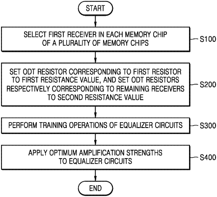
in response to a selection control signal, selecting a receiver from a plurality of receivers of each memory chip of a plurality of memory chips included in the memory device as a first receiver, wherein the plurality of memory chips share a plurality of data signal lines, wherein each memory chip includes a plurality of on-die termination (ODT) resistors, and the plurality of ODT resistors are respectively connected to the plurality of receivers of each memory chip;
in response to mode register setting command signals, setting each ODT resistor which is connected to a first receiver to a first resistance value, and setting ODT resistors which are connected to receivers which are not first receivers to a second resistance value; and
setting an amplification strength of an equalizer circuit of each first receiver by performing training operations,
wherein each data signal line of the plurality of data signal lines is respectively connected to a first receiver.
|