| CPC G11C 16/14 (2013.01) [G11C 5/06 (2013.01); G11C 16/0483 (2013.01); G11C 16/16 (2013.01); G11C 16/24 (2013.01); G11C 16/26 (2013.01); G11C 16/30 (2013.01)] | 13 Claims |
|
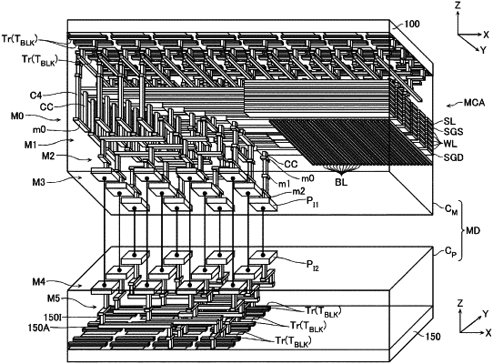
1. A semiconductor storage device comprising:
a first semiconductor substrate having a first active region;
a second semiconductor substrate having a second active region;
a first memory cell and a second memory cell provided between the first semiconductor substrate and the second semiconductor substrate;
a first word line electrically connected to a gate of the first memory cell;
a second word line electrically connected to a gate of the second memory cell;
a first transistor that is provided on the first semiconductor substrate and has a channel region thereof in the first active region, the first transistor having a first source and a first drain that are electrically connected between the first word line and a first wiring, the first transistor configured to control supply of a voltage from the first wiring to the gate of the first memory cell through the first word line; and
a second transistor that is provided on the second semiconductor substrate and has a channel region thereof in the second active region, the second transistor having a second source and a second drain that are electrically connected between the second word line and a second wiring, the second transistor configured to control supply of a voltage from the second wiring to the gate of the second memory cell through the second word line.
|