| CPC G11C 15/04 (2013.01) | 12 Claims |
|
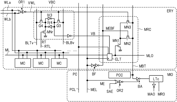
1. A semiconductor device having a CAM (Content Addressable Memory) unit,
wherein the CAM unit comprises:
a plurality of CAM entries;
a plurality of search lines provided so as to be common to the plurality of CAM entries and to which search data from outside the semiconductor device are input; and
a common match output line provided so as to be common to the plurality of CAM entries,
each of the plurality of CAM entries has:
a plurality of CAM cells configured to discriminate a match or mismatch between stored data stored in advance and the search data;
a match line coupled to the plurality of CAM cells, and having a voltage level controlled based on discrimination results of the plurality of CAM cells; and
a first transistor and a second transistor coupled in series between the common match output line and a predetermined power source,
the first transistor is controlled to be turned ON or OFF based on the voltage level of the match line,
the second transistor is controlled to be turned ON or OFF by a search enabling signal asserted at a time of a search operation, and
each of the plurality of CAM entries further has a third transistor coupled in parallel to the second transistor, and being controlled to be turned ON or OFF at a time of a read operation and based on a voltage level of a word line coupled to its own CAM entry.
|