| CPC G09G 3/3233 (2013.01) [H10K 59/131 (2023.02); G09G 2300/0426 (2013.01); G09G 2330/00 (2013.01)] | 23 Claims |
|
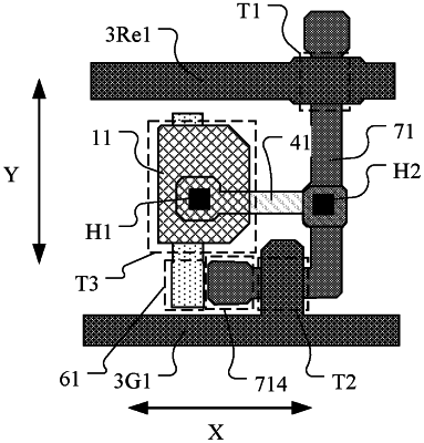
1. A display panel comprising a pixel driving circuit, wherein the pixel driving circuit comprises a driving transistor, a first transistor and a second transistor, a gate electrode of the first transistor is connected to a first gate line, a first electrode of the first transistor is connected to gate electrode of the driving transistor, a gate electrode of the second transistor is connected to a second gate line, a first electrode of the second transistor is connected to the gate electrode of the driving transistor, and a second electrode of the second transistor is connected to a second electrode of the driving transistor, the driving transistor is a P type transistor, the first and second transistors are N type transistors, and the display panel further comprises:
a base substrate;
a first conductive layer, disposed at a side of the base substrate and comprising a first conductive part, wherein the first conductive part is configured to form the gate electrode of the driving transistor;
a third conductive layer, disposed at a side of the base substrate and comprising the first gate line and the second gate line, wherein an orthographic projection of the first gate line on the base substrate and an orthographic projection of the second gate line on the base substrate are both extended in a first direction, and an orthographic projection of the first conductive part on the base substrate is positioned between the orthographic projection of the first gate line on the base substrate and the orthographic projection of the second gate line on the base substrate; and
a first connecting part, connected to the first conductive part via a through hole, and connected to the first electrode of the first transistor and the first electrode of the second transistor,
wherein an orthographic projection of the first connecting part on the base substrate is positioned between the orthographic projection of the first gate line on the base substrate and the orthographic projection of the second gate line on the base substrate.
|