| CPC G09G 3/3233 (2013.01) [G09G 3/2003 (2013.01); H10K 59/1213 (2023.02); G09G 2300/0426 (2013.01); G09G 2300/0452 (2013.01); G09G 2300/0866 (2013.01); G09G 2320/0209 (2013.01); G09G 2320/0219 (2013.01); G09G 2320/0223 (2013.01); G09G 2320/0233 (2013.01); G09G 2320/043 (2013.01); G09G 2330/025 (2013.01)] | 20 Claims |
|
1. A display unit comprising:
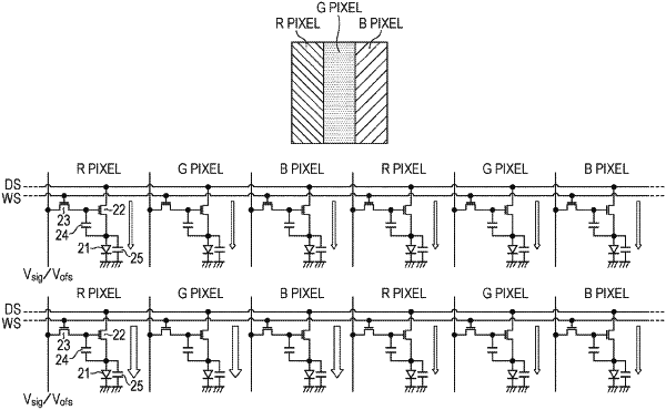
a plurality of pixels, respective ones of the plurality of pixels consisting of first, second, third and fourth sub-pixels including an R sub-pixel, a G sub-pixel, a B sub-pixel and a W sub-pixel, respective ones of the sub-pixels each including a light emitting element, a capacitor, a first transistor configured to write a signal potential to the capacitor, and a second transistor configured to provide a drive current to the light emitting element based on a voltage stored in the capacitor, the capacitor including a first terminal connected to a gate of the second transistor and a second terminal connected to a source or drain of the second transistor,
wherein the first transistor of each of the sub-pixels has a width-to-length ratio W/L, and
a width to length ratio W1/L1 of the first transistor of the first sub-pixel is different than a width-to-length ratio W2/L2 of the first transistor of the second sub-pixel.
|