| CPC G09G 3/32 (2013.01) [G09G 2300/0426 (2013.01); G09G 2300/0819 (2013.01); G09G 2300/0852 (2013.01); G09G 2310/00 (2013.01); G09G 2320/0633 (2013.01); G09G 2330/028 (2013.01)] | 17 Claims |
|
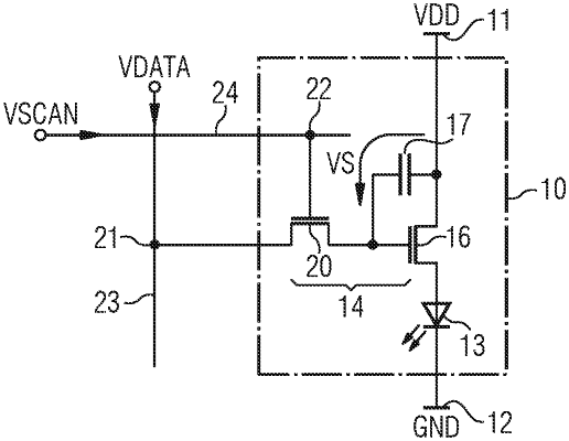
1. An image element, comprising
a first and a second supply terminal,
a light emitting semiconductor component,
a driver circuit comprising a driver transistor, a storage capacitor and a switching transistor, and
a trigger circuit comprising an output transistor and a control capacitor,
wherein the light emitting semiconductor component and the driver transistor are arranged in series with each other and between the first supply terminal and the second supply terminal,
wherein a first electrode of the storage capacitor is coupled to a control terminal of the driver transistor,
wherein the switching transistor is configured to switch on and off a current flow through the light emitting semiconductor component,
wherein a first electrode of the control capacitor is connected to a control terminal of the output transistor, and
wherein a first terminal of the output transistor is connected to a control terminal of the switching transistor.
|